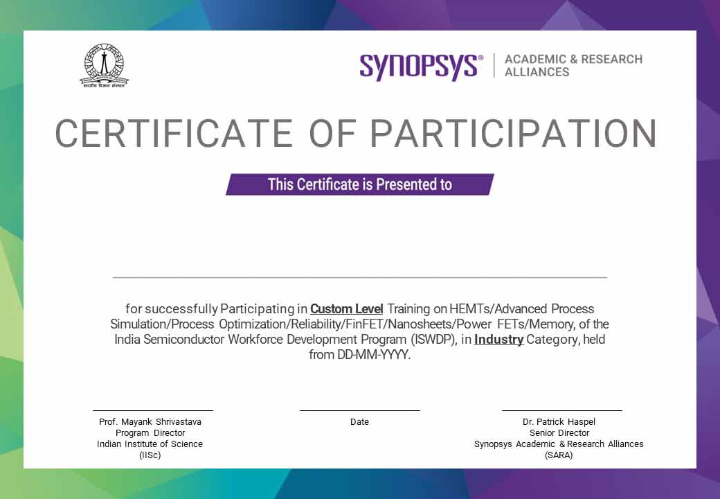
Advanced Process Simulation
To make the device structures industry relevant, this module will introduce following sub-modules:
- Significance of 3D simulation
- Virtualizing the manufacturing process
- Switching From 2D to 3D
- Defining 3D simulation domain
- Process Flow
- Efficient meshing strategy
- Doping mechanism and Structure-modifying steps (etching, deposition, photo, and transform)
- Visualization of devices in 3D,2D cutplanes and 1D cutlines
- Mask-based process simulation with direct import of GDSII layouts, 2D vs 3D
Process Optimization
This module comprises of following sub-modules:
- Deeper understanding of process parameters and models of ion implantation, diffusion, etching, and deposition
- Correlating the process parameter-device structure-device performance
- Process-aware Designing
- Optimization of existing processes to allow performance prediction
- Introducing parameter database browser
- Changing parameters in the command file
- Custom calibration.
Reliability
This module comprises of following sub-modules:
- Importance of predicting reliability
- Physics of various reliability models, NBTI, TCAD Degradation models - NBTI model, Hot Carrier model, Trap degradation model, Device lifetime and simulation
- Simulation Hands-on
FinFET & Nanosheets
This module comprises of following sub-modules:
- Technology scaling roadmap
- FinFET architecture
- TCAD Simulation of Double Gate, Triple Gate FinFETs
- Simulate various devices in FinFET Technology
- Understand the effect of device variation on the device performance
- Optimization guidelines
- Beyond FinFET technologies – Vertically stacked Nanosheet Technology
Power FETs
This module comprises of following sub-modules:
- Generating power MOSFET structures using process simulations
- Steps to carry out analysis of power MOSFETs
- Power MOSFET simulations in the presence of thermal effects
- Breakdown analysis
Memory
This module comprises of following sub-modules:
- Generating memory device structures in TCAD
- Capturing the processes leading to memory effect in the device
- Running transient simulations to understand the data storage time and date-retention capability
- Carrying out device analysis to optimize the memory performance
HEMTs
Industry Professionals will learn how to carry out simulations of HEMT devices. The module will comprise of following sub-modules:
- Building up basic device structure
- Carrying out calibration for DC and RF performance
- Identification and explanation of different physical models necessary to simulate DC behavior
- Analysis of the impact of epitaxial layer arrangement on the channel charge
- Simulating the Id-Vd and IdVg behavior of the device
- Enabling trap analysis in GaN HEMT device. Identification of critical parameters to be analyzed.
- OFF-state breakdown analysis of the devices
- Simulating the RF performance of the device
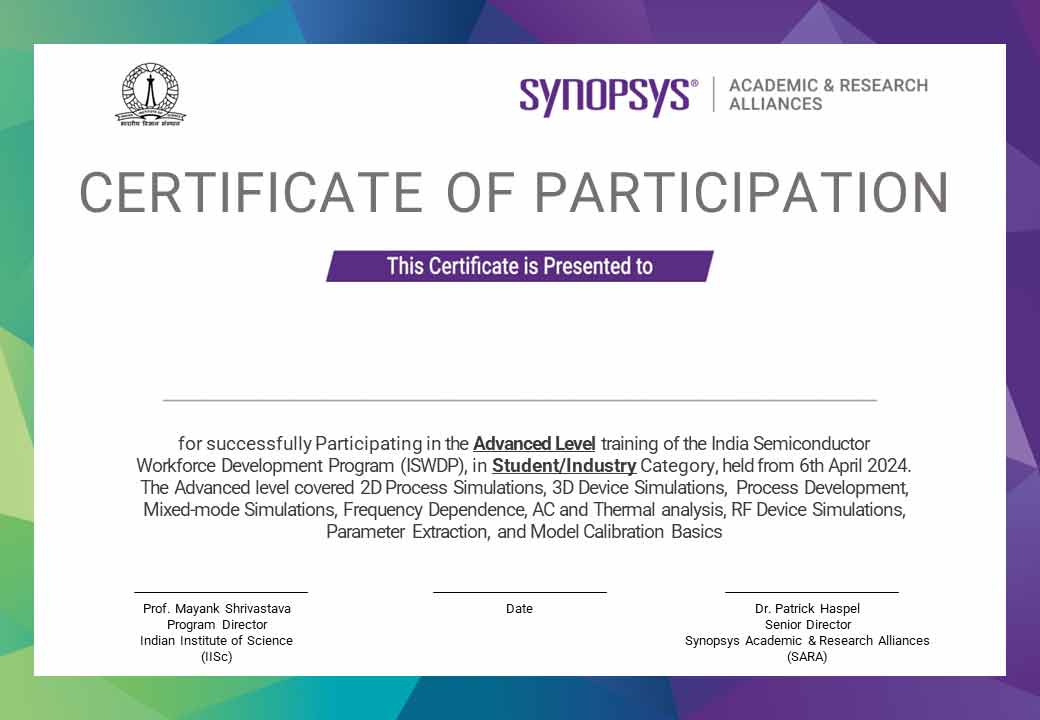
Advanced Emulations
We take the structure creation to advanced level by including following steps:
- Developing 3-D structures
- Meshing strategy for 3-D structures
- Defining doping profiles in 3-D structures
- Capturing essential device topologies, curves, edges and cornerns in 3-D structures
Device Calibration
On the device characteristics simulation front, we introduce the most important step to make the analysis relevant for industrial/research purposes. This will be accomplished with the help of following sub-modules
- Bringing structure as close as possible to real world scenario
- Learning basics of calibration
- Outlining steps for calibration of silicon based devices
- Learning how to select physical model for calibration
- Identifying different operating regimes in the output and transfer curves
- Identifying critical parameters of device physics models affecting device behavior in these operating regimes
Advanced Analysis
Detailed device analysis to be carried out in the following operating regimes:
- Carrying out Dc analysis
- Output characteristics
- Transfer characteristics
- Basic breakdown analysis
- AC analysis
- RF analysis
- Thermal analysis
- Learning how to position the thermodes
- Defining thermal boundary conditions and thermal resistances
- Determining temperature bsaed models to be accounted for thermal analysis of the device
- Analyzing heat distribution and critical areas for heat dissipation in the device
- Analysing I-V behavior under thermal considerations
Emulating Circuits
Leveling up on the simulation capabilities, this module will introduce the students to the following:
- Introduction to mixed mode simulations to enable device analysis in circuit scenarios. Basic circuits, like, inverter will be covered
- Analysing impact of circuit parasitics on device behavior
- Analysing impact of device paramters on circuit performance
Parameter Extraction
Simulations generate huge volumes of data which increases exponentially with size of the design of experiments. Parameter extraction enables one to extract the most important and relevant parameters from the simulation output to enable quick visualisation and comparison. In this module, you will learn
- To write scripts for automated data plotting
- Introduction to important functions including functions for extracting threshold voltage, on resistance, on current, saturation current, and breakdown voltage
- Introduction to building custom scripts for extracting custom parameters as per requirement.
Process Design
At this level, we move one more step closer to the real-world device structures with the help of following steps:
- Process simulations to factor in impact of process variations
- Complete layout based process flow emulation of practical device structures
- Analyzing impact of process conditions on critical device features like doping profile, junction depths, etc.
- Analyzing impact of anisotropic/isotropic etching
- Learning advanced meshing to properly capture doping variations
Design Automation
This module deals with the following:
- Script based device structure creation
- Learning to build the complete structure using critical design varibales
- Creating multiple variants of the device structure based on variation in geometrical parameters with the help of scripts
Deeper Insights
On the device simulation front at this level, we will be advancing the understanding of simulation by including following steps:
- Explanation of physical models used in estimating device behavior
- Playing with physical models to understand their impact on electrical characteristics of the device
Technology Relevant Design
What to expect:
- Replicating realistic device dimensions
- Building realistic doping profiles
- Enacpsulating gemometrical effects like overlaps
Outcome:
- Preparing realistic device structure and know the intricacies involved in defining doping profiles
Advanced Devices
At this level, we will be dealing with next level of sophistication in device structures, including the following:
- Device structures to be created : pMOS and CMOS
- Emulate process level variations in geometrical device structure creation tool
- Creating a complete CMOS structure taking into account device isolation strategy
First Cut Design
This modules deals with porting from building device structure to simulating device characteristics Students will learn,
- How to carry out basic simulations for estimating output and transfer characteristics of the structure developed through GUI
- How to generate family of curves
Basic Devices
At this level, the following two and three terminal device structures will be discussed
- Diodes
- BJTs
- MOSFETs
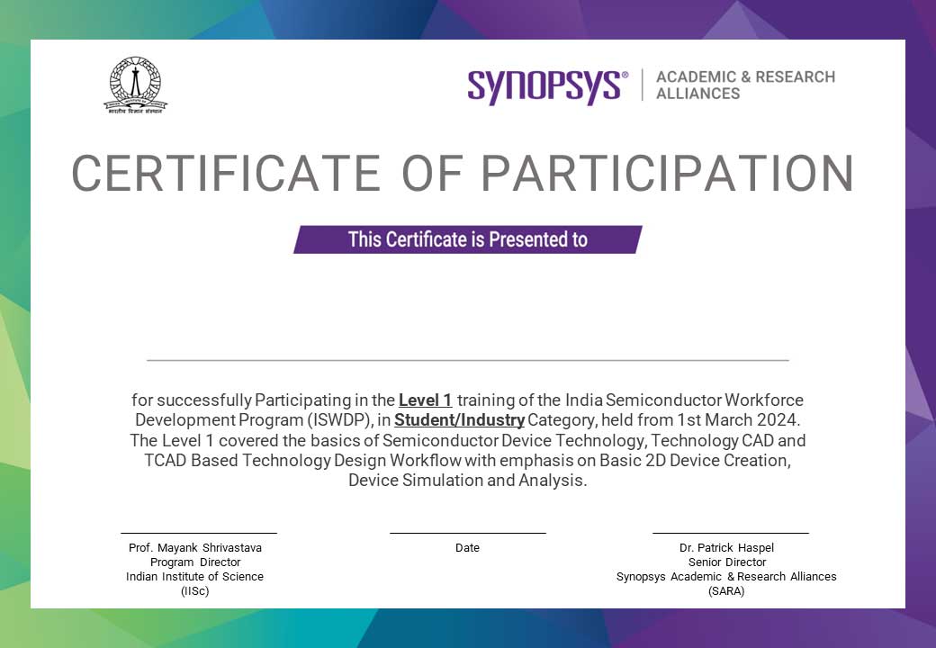
Text Books to TCAD
In this module, students will get to know how to draw basic device structures in TCAD and define doping profiles. This includes the following content
- Steps to create a basic device strcuture from scratch using GUI?
- Defining standard/idealized doping profiles
- Creating standard mesh


