Slide1

India Semiconductor Workforce Development Program

Shaping the Global Semiconductor Landscape: India Leads with Innovation and Expertise.
Collaborate, Innovate, and Transform with the India Semiconductor Workforce Development Program.
Slide2

India Semiconductor Workforce Development Program

Date: Feb 15 th - 16 th, 2024
Learn to Design, Model, Simulate & Develop Semiconductor Devices In Association with Prof. Mayank Shrivastava’s Nano Devices Lab (MSDLab), IISc Bangalore
Register Now Programme

The India Semiconductor Workforce Development Program: A Beacon for the Global Semiconductor Landscape

In the era of rapid technological advancement, the significance of semiconductors is paramount. They're not just the lifeblood of our digital devices, but they also play a crucial role in the innovation, development, and deployment of next-generation technologies. Recognizing this, the collaboration between the illustrious Indian Institute of Science (IISc) and Synopsys has culminated in the creation of the India Semiconductor Workforce Development Program (ISWDP). But what exactly is this program, and why is it vital not just for India, but for the world?

01 - What is the India Semiconductor Workforce Development Program (ISWDP)?

The India Semiconductor Workforce Development Program (ISWDP) is a unique and comprehensive initiative tailored to bridge the process technology and device design skill gap in the swiftly expanding semiconductor sector. It's a meticulously designed course, covering the foundations, diving deep into the nuances of device/technology development skills, and offering a hands-on approach through a microelectronics lab experience. Beyond the core curriculum, the program provides an unparalleled practical experience, offering students and industry professionals the chance to work on state-of-the-art research and development tools that are used by the semiconductor industry for semiconductor device and technology development.

Furthermore, ISWDP also bridges the gap between academic theories and real-world applications. The curriculum is crafted to overwhelm and fascinate participants to pursue a career in semiconductors, to think beyond textbooks, and to understand the intricacies involved in the development of 
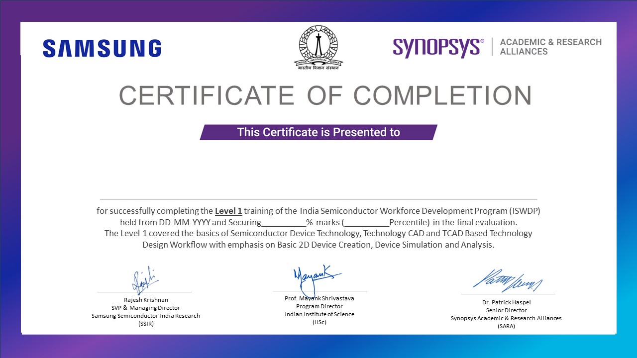
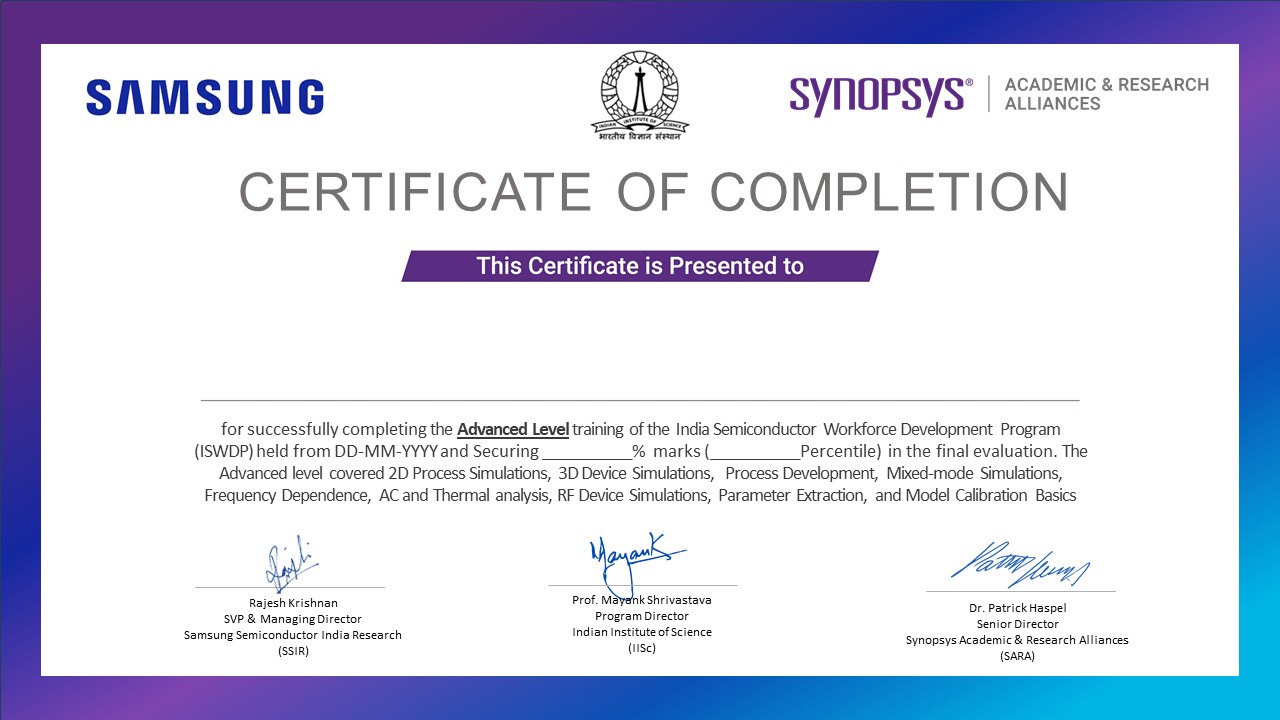
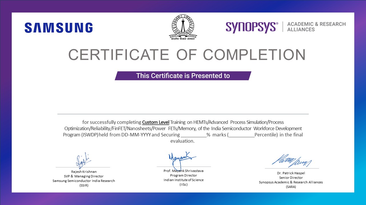
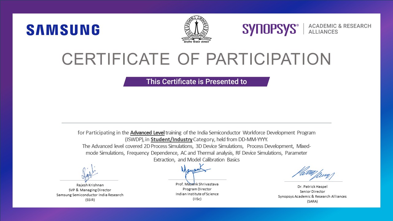
semiconductor technology. The live virtual program comprises four levels, i.e., Level 1, Level 2, Advance, and Custom. Launched in March 2024, the program runs 4 cohorts throughout the year (view the schedule here: https://iisc-iswdp.org/schedule.php. The program has successfully completed two cohorts with over 600 participants from both industry and academia.

03- Our Objectives

The India Semiconductor Workforce Development Program is strategically designed to achieve critical goals that support both the growth of India's semiconductor industry and the global technological landscape:

Developing Skilled Professionals: At the core of our mission is the commitment to cultivate a robust pipeline of skilled and highly inspired professionals. Through innovative education that blends rigorous academic coursework with practical, hands-on training, and active industry collaboration, we aim to equip participants with the advanced skills necessary to drive forward India’s semiconductor industry. Our comprehensive approach ensures that graduates are not only knowledgeable but also capable of contributing to and leading in a highly competitive field.

Cultivating Future Leaders: We are dedicated to inspiring and preparing the next generation for a future in semiconductors—this includes students, faculty, engineers, and professionals. Our program is designed to foster expertise, encourage innovation, and develop the skills necessary for global leadership. By exposing participants to the frontiers of semiconductor technology and its applications, we aim to ignite a lifelong passion for this dynamic field, setting them on a path to becoming pioneers of technological advancement.

Bridging Talent Gaps: A key objective of ISWDP is to serve as a bridge between industry demands and academic output. Having closely worked with semiconductor fabs and various development centers, we have identified the specific skills and capabilities required by the industry. Our program is tailored to prepare individuals who not only meet these requirements but are also primed for further training and specialization. Together, these objectives underscore our dedication to enriching the semiconductor ecosystem with talented individuals who are prepared to innovate, lead, and excel at a global level.

05- Benefits for Industries and Academic Institutions

The India Semiconductor Workforce Development Program (ISWDP) is a cornerstone for individuals and institutions aiming to excel in the semiconductor industry. It offers an avenue to delve deep into semiconductor technology, equipping participants with both foundational and advanced knowledge. This comprehensive program, supported by IISc and industry leaders such as Synopsys, offers a multifaceted approach to learning, blending academic rigor with practical industry insights. Whether you're a fresh graduate or an industry professional, the program offers something for everyone, ensuring a clear path to leadership in the semiconductor domain

A. For Students:

The program won't just teach; it will inspire. It will encourage students to visualize the processes and to connect the dots between what they learn and how it applies in the industry. It gives practical experience in semiconductor design and process, preparing the students to tackle industry challenges immediately upon graduation. The program benefits students through:

  • Hands-On Learning: Students engage with advanced computational tools like TCAD (Technology Computer-Aided Design), providing a real-world grasp of semiconductor design and process.
  • Industry-Relevant Skills: The curriculum covers the entire gamut of semiconductor development, from fundamental concepts to complex device processes and device design techniques, ensuring that students are well-prepared for the industry.
  • Real-World Application: The integration of theoretical knowledge with practical applications allows students to experience and solve real semiconductor problems.
  • Internship Opportunities: Students can access merit-based internships in both virtual and physical formats, complete with certifications, enhancing their practical experience and industry relevance.
  • Project Implementation: The program encourages students to propose and implement their projects, fostering creativity and problem-solving skills.

B. For Aspiring Professionals:

For those already in the field or looking to enter, ISWDP, when participants credit all the offered levels, provides tools and experiences to deepen their expertise and advance their careers:

  • Interactive Sessions: : Led by experts, these sessions delve into the complexities of semiconductor processes, enhancing understanding and sparking curiosity
  • Problem-Solving Workshops:: Participants tackle industry-relevant scenarios that hone their analytical and problem-solving skills, preparing them for real-world challenges.
  • Exposure to Industry Practices: Our collaborations with leading technology companies enable participants a firsthand look at the semiconductor industry’s practices, challenges, and innovations.
  • Custom Modules: : Thanks to growing industry interest, ISWDP offers custom modules on specialized topics like Fabrication, Characterization, and Packaging at no additional cost, ensuring that learning is continually updated and relevant.

C. For Academic Institutions

Academic institutions can reap numerous benefits by participating in ISWDP. The program offers substantial educational opportunities and unique advantages that enhance its curriculum and reputation for its generations of students. These include:

  • Bulk Registrations: Institutions benefit from attractive discounts on bulk registrations, making advanced education more accessible to their students.
  • New Technical Offerings: : The program continuously expands its offerings, introducing Custom modules sponsored by prominent industry players starting from Cohort 3 in September 2024.
  • Internship Opportunities: Institutions can facilitate merit-based internships for their students, providing valuable industry exposure and experience.
  • Certificates of Appreciation: Institutions supporting and encouraging their students to pursue a career in semiconductors receive acknowledgment certificates from the program, enhancing their prestige and demonstrating their commitment to cutting-edge technological education.

D. A Boost for Industries

The global semiconductor shortage presents not only a workforce gap but also a broad supply chain and production challenge. By equipping a new generation of engineers with the necessary skills, ISWDP helps industries innovate faster, maintain higher quality standards, and find quicker solutions to complex problems, thereby enhancing the overall health and capacity of the semiconductor industry.

08- Join Now (as a Participant)

Join us to start your journey in mastery, innovation, and global leadership as we together shape the future of technology and create a new legacy of Indian engineering excellence in semiconductors.

Register now at: https://iswdp.registeryourseat.in

02- Our Vision

The India Semiconductor Workforce Development Program (ISWDP) aims to position India at the forefront of the global semiconductor industry. Our vision extends beyond technological advancement; we aspire to spark a national enthusiasm for semiconductors, paralleling the excitement surrounding fields like artificial intelligence and computer science. Through ISWDP, we are committed to transforming education by seamlessly integrating academic knowledge with real-world industry demands. This approach not only enriches learning but also prepares a new generation of engineers and technologists to lead and innovate within the global semiconductor landscape.

We are dedicated to creating educational experiences that are not just informative but truly transformative, enabling students and professionals to grasp the intricacies of semiconductor technologies and their applications. Our program is crafted to inspire curiosity and drive innovation, ensuring that participants are well-equipped to contribute to and lead in the rapidly evolving tech world.

For a deeper understanding of our ambitious vision and the strategic expansion plans set to unfold over the next few years, we invite you to read the detailed interview published by Electronics For You: https://www.electronicsforu.com/technology-trends/interviews/we-intend-to-expose-5000-people-to-chip-design-development-manufacturing-processes-in-three-years.

04- Role of ISWDP in Mitigating the Global Semiconductor Shortage by Boosting India's Presence

Semiconductors are the cornerstone of modern technology, indispensable across sectors from consumer electronics to national defense systems. In recent years, the global demand for skilled semiconductor professionals has surged as technology becomes increasingly integral to our lives and industries. This escalating demand, coupled with India's proactive strides in semiconductor fabrication and manufacturing, underscores the critical need for initiatives like the India Semiconductor Workforce Development Program (ISWDP). It’s worth highlighting that the ISWDP isn't merely a reactionary measure to the current global semiconductor workforce shortage; it's a forward-thinking solution that prepares India to meet both current and future challenges in the semiconductor sector. By 2030, the program is poised to significantly bolster the pool of skilled professionals, ready to address and propel the global semiconductor landscape.

Leveraging the Indian Institute of Science's (IISc) century-long legacy of academic excellence and its distinction as an Institute of Eminence, the ISWDP is uniquely positioned to nurture exceptional talent. This talent development is aligned with the needs of semiconductor fabs in India, reducing dependency on international imports and enhancing domestic capabilities. The program’s curriculum is meticulously designed to provide undergraduate and postgraduate students with practical, hands-on training in semiconductor process and device design skills required in semiconductor product development. Moreover, The ISWDP is committed to doing more than just filling jobs or training engineers; it aims to cultivate the next generation of leaders who will drive India to a prominent position in the competitive global semiconductor industry. This commitment has gained renewed vigor following recognition and support from the Honorable Minister of Electronics and Information Technology, Government of India. With this endorsement, the ISWDP is more dedicated than ever to providing comprehensive training to students and professionals, ensuring they are well-prepared to meet the demands and challenges of the semiconductor industry.

06- Impact on Society: Catalyzing Change through Semiconductor Excellence

The India Semiconductor Workforce Development Program (ISWDP) transcends the traditional boundaries of an educational initiative; it embodies a national movement poised to elevate India to a leading position in the global semiconductor landscape. This visionary program does more than impart technical knowledge—it inspires societal transformation and economic revitalization.

Economic Growth: ISWDP will become a crucial pivot point for India’s economic strategy. By nurturing a homegrown talent pool skilled in high-tech semiconductor production, the program would directly boost India’s economic resilience. As these professionals enter the workforce, their expertise will enable the expansion of domestic semiconductor manufacturing capabilities, reducing the nation's dependency on semiconductor imports. This shift not only supports the local economy but also positions India as a critical player in the global supply chain, attracting foreign investment and fostering technological advancements

Innovation Ecosystem: The ripple effects of ISWDP will be profoundly felt within the innovation ecosystem. Graduates from the program will not just be skilled in semiconductor processes and design principles; they will also be inspired to eventually become pioneers of future technology. Trained to acquire cutting-edge knowledge and practical skills, the spark that we produce is expected to lead them toward taking charge of developing new technologies and innovative solutions. The contributions of these inspired graduates would be the key to addressing some of the most pressing global challenges, from sustainable energy solutions to advanced information technologies, thereby reinforcing India's status as a hub of technological innovation.

National Security: Strengthening India’s semiconductor capabilities has strategic implications beyond economics and innovation; it is pivotal to national security. In an era where technology underpins much of our defense infrastructure, having a robust, self-sufficient semiconductor industry safeguards India’s technological sovereignty. This strategic autonomy is critical in maintaining security and gives the nation a competitive edge on the global stage.

07- Why Now? Seizing the Semiconductor Renaissance

The global semiconductor industry is currently experiencing a dynamic renaissance. These tiny yet powerful components are crucial in powering everything from our everyday smartphones to groundbreaking technologies like artificial intelligence and quantum computing. This surge in demand and utility marks the current decade, 2020-2030, as the "decade of semiconductors."

Strategic Timing for a Strategic Move: : India stands at a pivotal moment in its technological evolution. With its strategic positioning and growing capabilities in the semiconductor sector, coupled with increasing demand from a diverse range of industries, India is on the cusp of becoming a global leader in this critical market. The timing could not be more opportune for such an initiative as the India Semiconductor Workforce Development Program (ISWDP).

Driving Factors for the Urgency of ISWDP

  • Technological Advancements: : As technologies evolve at an unprecedented rate, the dependency on semiconductors continues to escalate. This is not just in terms of quantity but also in the complexity and capability of semiconductor technology required to drive these innovations.
  • Market Demand: The demand for more sophisticated semiconductor components is booming across various sectors, including telecommunications, automotive, healthcare, and consumer electronics. This demand is not just a temporary surge but a long-term trend that will shape the future of these industries.
  • National Economic Strategy: For India, developing a strong semiconductor industry is not just about meeting domestic or global demand. It's about establishing a strategic industry that can enhance economic stability, reduce dependence on imports, and position India as a hub of innovation and manufacturing in the global economy.
  • Skilled Workforce Development: There is a critical need for skilled professionals who can not only understand the intricacies of semiconductor process and design but also innovate and improve upon existing technologies. ISWDP aims to fill this gap, ensuring that India has a ready pool of talented individuals to lead and support this burgeoning sector.

Advanced Process Simulation

To make the device structures industry relevant, this module will introduce following sub-modules:

  1. Significance of 3D simulation
  2. Virtualizing the manufacturing process
  3. Switching From 2D to 3D
  4. Defining 3D simulation domain
  5. Process Flow
  6. Efficient meshing strategy
  7. Doping mechanism and Structure-modifying steps (etching, deposition, photo, and transform)
  8. Visualization of devices in 3D,2D cutplanes and 1D cutlines
  9. Mask-based process simulation with direct import of GDSII layouts, 2D vs 3D

Process Optimization

This module comprises of following sub-modules:

  1. Deeper understanding of process parameters and models of ion implantation, diffusion, etching, and deposition
  2. Correlating the process parameter-device structure-device performance
  3. Process-aware Designing
  4. Optimization of existing processes to allow performance prediction
  5. Introducing parameter database browser
  6. Changing parameters in the command file
  7. Custom calibration.

Reliability

This module comprises of following sub-modules:

  1. Importance of predicting reliability
  2. Physics of various reliability models, NBTI, TCAD Degradation models - NBTI model, Hot Carrier model, Trap degradation model, Device lifetime and simulation
  3. Simulation Hands-on

FinFET & Nanosheets

This module comprises of following sub-modules:

  1. Technology scaling roadmap
  2. FinFET architecture
  3. TCAD Simulation of Double Gate, Triple Gate FinFETs
  4. Simulate various devices in FinFET Technology
  5. Understand the effect of device variation on the device performance
  6. Optimization guidelines
  7. Beyond FinFET technologies – Vertically stacked Nanosheet Technology

Power FETs

This module comprises of following sub-modules:

  1. Generating power MOSFET structures using process simulations
  2. Steps to carry out analysis of power MOSFETs
  3. Power MOSFET simulations in the presence of thermal effects
  4. Breakdown analysis

Memory

This module comprises of following sub-modules:

  1. Generating memory device structures in TCAD
  2. Capturing the processes leading to memory effect in the device
  3. Running transient simulations to understand the data storage time and date-retention capability
  4. Carrying out device analysis to optimize the memory performance

HEMTs

Industry Professionals will learn how to carry out simulations of HEMT devices. The module will comprise of following sub-modules:

  1. Building up basic device structure
  2. Carrying out calibration for DC and RF performance
  3. Identification and explanation of different physical models necessary to simulate DC behavior
  4. Analysis of the impact of epitaxial layer arrangement on the channel charge
  5. Simulating the Id-Vd and IdVg behavior of the device
  6. Enabling trap analysis in GaN HEMT device. Identification of critical parameters to be analyzed.
  7. OFF-state breakdown analysis of the devices
  8. Simulating the RF performance of the device

Advanced Emulations

We take the structure creation to advanced level by including following steps:

  1. Developing 3-D structures
  2. Meshing strategy for 3-D structures
  3. Defining doping profiles in 3-D structures
  4. Capturing essential device topologies, curves, edges and cornerns in 3-D structures

Device Calibration

On the device characteristics simulation front, we introduce the most important step to make the analysis relevant for industrial/research purposes. This will be accomplished with the help of following sub-modules

  1. Bringing structure as close as possible to real world scenario
  2. Learning basics of calibration
    1. Outlining steps for calibration of silicon based devices
    2. Learning how to select physical model for calibration
    3. Identifying different operating regimes in the output and transfer curves
    4. Identifying critical parameters of device physics models affecting device behavior in these operating regimes

Advanced Analysis

Detailed device analysis to be carried out in the following operating regimes:

  1. Carrying out Dc analysis
    1. Output characteristics
    2. Transfer characteristics
    3. Basic breakdown analysis
  2. AC analysis
  3. RF analysis
  4. Thermal analysis
    1. Learning how to position the thermodes
    2. Defining thermal boundary conditions and thermal resistances
    3. Determining temperature bsaed models to be accounted for thermal analysis of the device
    4. Analyzing heat distribution and critical areas for heat dissipation in the device
    5. Analysing I-V behavior under thermal considerations

Emulating Circuits

Leveling up on the simulation capabilities, this module will introduce the students to the following:

  1. Introduction to mixed mode simulations to enable device analysis in circuit scenarios. Basic circuits, like, inverter will be covered
  2. Analysing impact of circuit parasitics on device behavior
  3. Analysing impact of device paramters on circuit performance

Parameter Extraction

Simulations generate huge volumes of data which increases exponentially with size of the design of experiments. Parameter extraction enables one to extract the most important and relevant parameters from the simulation output to enable quick visualisation and comparison. In this module, you will learn

  1. To write scripts for automated data plotting
  2. Introduction to important functions including functions for extracting threshold voltage, on resistance, on current, saturation current, and breakdown voltage
  3. Introduction to building custom scripts for extracting custom parameters as per requirement.

Process Design

At this level, we move one more step closer to the real-world device structures with the help of following steps:

  1. Process simulations to factor in impact of process variations
  2. Complete layout based process flow emulation of practical device structures
  3. Analyzing impact of process conditions on critical device features like doping profile, junction depths, etc.
  4. Analyzing impact of anisotropic/isotropic etching
  5. Learning advanced meshing to properly capture doping variations

Design Automation

This module deals with the following:

  1. Script based device structure creation
  2. Learning to build the complete structure using critical design varibales
  3. Creating multiple variants of the device structure based on variation in geometrical parameters with the help of scripts

Deeper Insights

On the device simulation front at this level, we will be advancing the understanding of simulation by including following steps:

  1. Explanation of physical models used in estimating device behavior
  2. Playing with physical models to understand their impact on electrical characteristics of the device

Technology Relevant Design

What to expect:

  1. Replicating realistic device dimensions
  2. Building realistic doping profiles
  3. Enacpsulating gemometrical effects like overlaps

Outcome:

  1. Preparing realistic device structure and know the intricacies involved in defining doping profiles

Advanced Devices

At this level, we will be dealing with next level of sophistication in device structures, including the following:

  1. Device structures to be created : pMOS and CMOS
  2. Emulate process level variations in geometrical device structure creation tool
  3. Creating a complete CMOS structure taking into account device isolation strategy

First Cut Design

This modules deals with porting from building device structure to simulating device characteristics Students will learn,

  1. How to carry out basic simulations for estimating output and transfer characteristics of the structure developed through GUI
  2. How to generate family of curves

Basic Devices

At this level, the following two and three terminal device structures will be discussed

  1. Diodes
  2. BJTs
  3. MOSFETs

Text Books to TCAD

In this module, students will get to know how to draw basic device structures in TCAD and define doping profiles. This includes the following content

  1. Steps to create a basic device strcuture from scratch using GUI?
  2. Defining standard/idealized doping profiles
  3. Creating standard mesh

India Semiconductor Workforce Development Program
Mode: Online

Contents

Tools

Details

Contents

Tools

Details

Contents

Tools

Details

Contents

(One of the Following)

Tools

Details

TIME LEFT FOR THE Next COHORT
Date: 1st October 2024

Our Sponsors

Please reach out to Dr. Nimitha, Program Manager, to express your interest in supporting or sponsoring the program ( nimithap@iisc.ac.in )